ChipX –
Launch Your
Semiconductor Career
A career-defining program designed to turn fresh graduates and early-career engineers into industry-ready semiconductor professionals. Learn directly from expert mentors through hands-on labs, live lectures, and real-world chip design projects that mirror the workflows of global semiconductor giants.
PG Program in
Semiconductor - Specialization in Physical Design
An overview
PG Program in Semiconductor
Specialization in Physical Design
A 6-Month Masterclass | India’s First Dedicated Semiconductor School
Why Physical Design (PD)?
In today’s $1T global semiconductor industry, Physical Design Engineering is one of the most in-demand roles. Every chip — from smartphones to AI processors — goes through the PD stage before manufacturing.
For ECE graduates, this is the fastest-growing career path in VLSI, offering high salaries, global opportunities, and cutting-edge work. With thousands of unfilled PD jobs in India alone, this is where the future is being built.
What You’ll Master at ChipX
- ⚡ Place & Route (PnR): Implement circuits on silicon with precision.
- ✅ Physical Verification (PV): Ensure designs meet manufacturing standards.
- ⏱ Static Timing Analysis (STA) & IR Drop Analysis: Guarantee performance & reliability.
- 📏 Sign-off Methodologies: Proven industry checks before fabrication.
- 🌀 Synthesis to GDSII Flow: End-to-end backend VLSI design training.
- 🛠 Hands-on with Synopsys, Cadence & Siemens EDA tools guided by experts.
Why ChipX PG Program is Different.
- 🔬 Real-Time Projects — industry-level designs, not just theory.
- 🏭 Industry Labs — real-world chip design workflows.
- 👨🏫 Mentorship — 10+ years of PD experience.
- 📂 Capstone Projects — build an industry-ready portfolio
- 💼 Placement-Ready — resume, interview prep & referrals.
- 🚀 Fast-Track Career — PD engineers earn up to ₹30 LPA in India.
- 🤝 Networking — connect with peers in Bengaluru’s VLSI hub.
Your Career Advantage
- 🎓 Eligibility: BTech / MTech / BE / ME - ECE, EEE, CSE, CS & IT, AI, VLSI freshers & early-career engineers (0–6 years exp.)
- ⏳ Duration: 6 months intensive
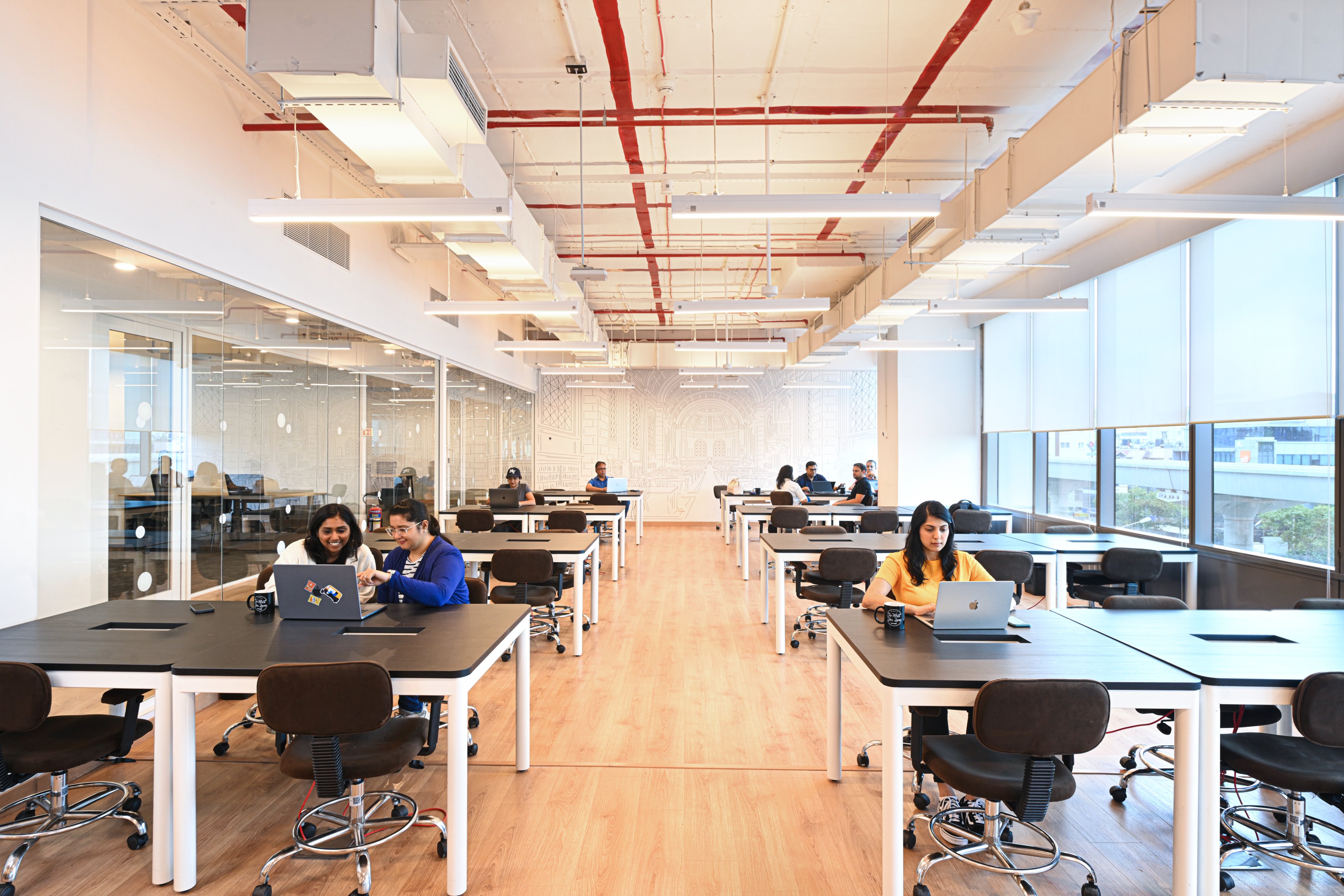
- 🏫 Mode: Hybrid (ChipX Campus @ WeWork Tech Hub, Marathahalli, Bengaluru)
- 🎯 Outcome: Become an industry-ready Physical Design Engineer
ChipX Physical Design Journey
At ChipX, every learner follows a structured, industry-grade journey — designed to transform fresh graduates into industry-ready Physical Design Engineers.
Phase 1: Foundations
Digital Electronics, VLSI CMOS & Network Theory, Basics of Physical Verification
Phase 2: Core Engineering Tools
Static Timing Analysis (STA Engineering), Linux for VLSI
Phase 3: Design Languages
Verilog for Logic Design, Tcl for Automation
Phase 4: Entry to Backend Flow
Input Files in PD, Logic Synthesis
Phase 5 – Phase 18: The Physical Design Flow
Floorplanning & Power Planning, Placement Optimization, Clock Tree Synthesis (CTS), Routing & ECO (Engineering Change Orders), Signoff Methodologies
Phase 18 – Phase 24: Advanced Physical Verification
Full-Time Physical Verification Practice, Advanced Design Rule Checks (DRC), Layout vs. Schematic (LVS)
Phase 24 Onwards: Career Prep & Industry Readiness
Mock Industry Projects, Resume & Portfolio Building, Semiconductor Industry Interviews & Placement Preparation
Outcome
By the end of the journey, ChipX engineers are interview-ready, tool-ready, and project-ready to contribute to India’s growing $5Bn+ semiconductor ecosystem.
ChipX PG Program: Application Journey
🚀 Admissions for Cohort 1 (2026) are now open! Apply early to secure your spot in India’s first dedicated PG Program in Semiconductor.
- Applications Review OpenNovember 2025
- Round 1 Deadline26th January 2026
- Round 2 Deadline23rd February 2026
- Round 3 Deadline23rd March 2026
- Final Application Close31st March 2026
- Program Kick-off6th April 2026
👉 Don’t miss the deadlines — limited seats for Cohort 1 (2026).
Your Application Process
✨ From application to admission, we make sure only the most motivated and talented engineers join the program.
- Straightforward and transparent process
- Guidance at every stage
- Personal interaction with mentors
- Selection focused on aptitude & passion
Semiconductor Courses
Physical Design Engineer Program
Master PD with ChipX and unlock cutting-edge skills for a future in advanced VLSI innovation.
Semiconductor Student Internship
ChipX Internship Program
2K+ Learners
Gain Hands-on Experience in VLSI with EDA Tools. Designed for aspiring VLSI engineers to gain real-world exposure. Focus on Physical Design Engineering with the latest industry projects. Flexible modes: Online & Hybrid options based on student location.
Internship Structure / Modules
- Weekdays: 1-hour faculty-led classes.
- Weekends: Access to ChipX Lab.
Highlights
- ✔ Learn from industry experts with 10+ years of experience.
- ✔ Practical exposure to the latest VLSI design trends.
- ✔ Opportunity to build projects for your resume & placements.
- ✔ Hands-on training using Synopsys EDA tools.

Physical Design Engineer Program (PD Engineer)
We make PD Engineers
1K+ Learners
Six months of extensive Physical Design Program for college students and pass out engineers.
Internship Structure / Modules
- Place & Route (PnR)
- Physical Verification (PV)
- Static Timing Analysis (STA) & IR drop analysis
- Sign-off methodologies
- Complete Synthesis to GDSII flow
- Soft Skills & Communication Skills
Highlights
- ✔ Master the complete PD flow from synthesis to GDSII
- ✔ Gain hands-on experience with real industry projects
- ✔ Learn essential soft skills and professional communication

Personality Development & Soft Skills
Top Non-Technical Program
3K+ Learners
As you need to be strong technically, you also need excellent communication and personality. ChipX provides a platform with top non-technical programs for engineers and students.
Accelerate Your
Semiconductor Career @ ChipX
ChipX PG Program is more than a course. It’s a launchpad into the semiconductor industry.
With our industry-validated curriculum, mentorship from global experts, and direct exposure to real projects, you’ll graduate job-ready to join companies like Intel, Qualcomm, Synopsys, Samsung, and MediaTek.
Upskill. Build. Lead the future of semiconductors with ChipX.
Applications now open for April 2026 — Selection through Screening & Interview only.